Blog
May 19, 2025
Integrating PLM with IPLM to Optimize IP Semiconductor Lifecycle Management

Embedded Systems & Chip Design
According to Deloitte, the semiconductor industry is on track to reach $1 trillion in annual sales by 2030. This rapid expansion—fueled by technological breakthroughs and relentless consumer demand—creates both opportunity and complexity. While traditional Product Lifecycle Management (PLM) is a mainstay of industries needing to manage product data, processes, and collaboration across the value chain, PLM systems don't always meet the unique challenges enterprise semiconductor organizations face.
Managing hectic and dynamic semiconductor workflows with hundreds or thousands of reusable IP blocks while working across multiple teams and meeting strict regulatory standards requires a more specialized approach. That’s where IP (intellectual property) Lifecycle Management (IPLM) comes in. Designed specifically for semiconductor organizations, IPLM complements and enhances PLM by offering a more specialized approach to IC and system design.
This guide explores how integrating PLM with IPLM optimizes processes, promotes collaboration, and alleviates the common semiconductor lifecycle roadblocks companies often face.
Back to top3 Challenges of Semiconductor PLM
PLM systems are used by the automobile industry, aerospace industry, industrial equipment segment, and financial services. However, when it comes to semiconductor design, fast-changing consumer demands and technological advancements have changed the playing field.
Here are three of the most common semiconductor design challenges with PLM and how integrating IPLM solves the issue:
1. Pace of Innovation
- Challenge: Semiconductors are designed in fast-paced environments where thousands of design files are checked out and in daily.
- Solution: To effectively manage your designs, you need to raise the level of abstraction from individual files to that of IP. By managing at the IP level, you can easily navigate complex hierarchical relationships and dependencies as single IPs. Utilizing IP management software minimizes oversight and improves efficiency, making it possible to keep pace with shifting industry and consumer trends.
2. Accelerated Lifecycles
- Challenge: Consumer demand for the latest technology fuels faster lifecycles. For example: users might upgrade their mobile phone every year or even more frequently.
- Solution: Instead of building from scratch, semiconductor companies can reuse IP and derivative designs to speed development. This requires an effective IP lifecycle management system that also tracks metadata for a fully transparent and traceable design process.
3. Information Siloes
- Challenge: Due to organizational structure or as a result of mergers and acquisitions, many companies have IP scattered across multiple design team siloes.
- Solution: Break down silos and make IPs universally accessible across design teams for more coordinated development workflows. This requires an all-in-one source of truth with carefully managed user permissions.
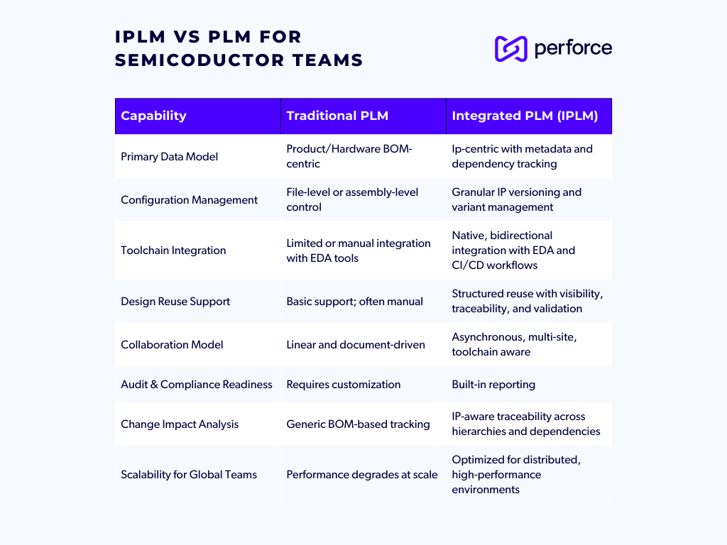
How IPLM Optimizes Semiconductor Product Lifecycle Management
IPLM is a semiconductor-specific evolution of traditional PLM that goes beyond managing hardware bill of materials (BOMs) and change orders. It brings deep support for IP governance, including versioning, traceability, and secure collaboration throughout the entire chip design and production lifecycle—from concept to tape-out and beyond.
In contrast to conventional PLM platforms, IPLM:
- Tracks and manages IP-centric data models
- Integrates seamlessly with Electronic Design Automation (EDA) tools
- Enables design reuse with confidence
- Supports industry compliance
Integrating these two solutions leads to streamlined and cost-efficient business processes and optimized semiconductor design. In this joint solution, the IPLM tool tracks the IP bill of information (BOI), which contains all IP in each design. This BOI can be fed forward into the PLM system to tie the engineering BOM and manufacturing BOM to the semiconductor design process.
In this way, manufacturing, legal, contracts, compliance, sales, and support have a view into what happens during design. Additionally, it keeps the other processes used by various departments updated with the latest information. You gain superior efficiency, decision making, and collaboration across teams.
Back to topWhy Choose Perforce IPLM as Your IP Design Lifecycle Tool
Perforce IPLM (formerly Helix IPLM) is the most efficient and effective IP lifecycle management platform for semiconductor organizations. It combines the power of integrated tools, secure collaboration, and advanced IP lifecycle management to help developers meet their challenges head on.
Perforce IPLM stands out with:
- Seamless Collaboration Across Teams: With Perforce IPLM, you can connect IP producers and consumers effortlessly. Whether your teams are working locally or across the globe, our IPLM platform ensures workflows are synchronized for smooth coordination and minimal disruptions.
- End-to-End IP Traceability: Gain full transparency into every stage of your IP lifecycle. With intuitive tracking tools, Perforce IPLM ensures that all IP and metadata is accounted for, making it easier to meet critical compliance regulations.
- Streamlined Integration with Existing Tools: Perforce IPLM is designed to work seamlessly with industry-standard data management solutions like Perforce P4. This eliminates the headaches of compatibility issues, enabling quicker adoption and smoother operations.
- Efficient Design Reuse: Accelerate development timelines by leveraging hierarchical IP management and a rich IP catalog. By enabling teams to reuse IP assets with ease, Perforce IPLM reduces redundancies, saving critical time and resources.
- Scalability for Global Development: Whether you’re a small team or a large, multi-site organization, Perforce IPLM scales effortlessly to support your needs. Its robust architecture is built to handle complex, asynchronous global collaboration without compromising performance or security.
- Enhanced IP Security: Protect your semiconductor assets when working with external partners by leveraging Perforce IPLM’s advanced security features. With precise user permissions and safeguarded data access, you maintain control over your intellectual property.
Don’t let your semiconductor design cycles lag. To learn more about integrating Perforce IPLM with your current PLM system for accelerated time-to-market, connect with one of our experts. We can walk you through the features and capabilities of Perforce IPLM, provide pricing information, and schedule a live demo geared towards your specific needs.