Blog
Insights, Innovations, and Best Practices from Perforce Experts
 Blog
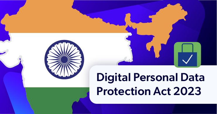
Blog How to Achieve India’s DPDP Compliance for Non-Production Data & AI Workflows
What are the best practices for DPDP compliance in the AI era? Perforce Delphix expert Sreevatsa Sreerangaraju explains the rules and tips for India’s Digital Personal Data Protection Act.
Data Management, Security & Compliance

 Blog
Blog Protecting Sensitive Data in Non-Production Environments: No Trade-Offs Necessary!
Learn why protecting sensitive data is critical, especially in non-production environments, and how to mitigate risks using effective masking techniques in this blog from Ann Rosen, Director of Product Marketing for Perforce Delphix.
Data Management, Security & Compliance

 Blog
Blog Perforce Delphix vs. Tonic: How to Choose the Right Solution for Synthetic & Test Data Management
See how Perforce Delphix stacks up against test data competitor Tonic — including a direct comparison of capabilities like synthetic data generation and data delivery. Delphix experts Woody Evans and Vikram Kulkarni break down the key differences and benefits.
Data Management, Security & Compliance, AI
 Blog
Blog Non-Negotiables in an Enterprise Synthetic Solution: #1, Referential Integrity
Referential integrity is a critical requirement for enterprise synthetic data. In this Q&A with Perforce Delphix expert Mayank Ahluwalia, learn why disconnected data relationships break testing, where most synthetic data tools fall short, and what capabilities organizations should evaluate to ensure synthetic and masked data work together across complex environments.
Data Management, DevOps
 Blog
Blog Perforce Delphix vs. DataMasque: How to Choose the Right Solution for Data Masking
Perforce Delphix vs. DataMasque — which can better protect your enterprise data? In this blog, Delphix experts Brian Muskoff and Bruce Liu break down each provider’s capabilities, features, and benefits for protecting and managing data.
Data Management, Security & Compliance
 Blog
Blog What’s Next in Perforce Intelligence: Building the Control Plane for Enterprise AI
In this update from Perforce CTO Anjali Arora, learn how Perforce Intelligence is evolving into a control plane for enterprise AI — helping organizations orchestrate, validate, and govern AI across the software development lifecycle. New capabilities address the challenges of scaling AI with control, visibility, and compliance.
AI, DevOps
 Blog
Blog Data Automation for Enterprise Innovation: 6 Challenges to Solve
There are 6 key challenges in legacy data automation. Get expert insights on where legacy ETL tools fail and how modern data automation transforms enterprise development from Nick Mathison, Senior Product Manager for Perforce Delphix.
DevOps, Data Management
 Blog
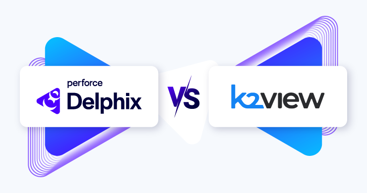
Blog Perforce Delphix vs. K2view for Test Data Management: How to Choose the Right Solution That Provides AI-Ready Data
Evaluate Delphix vs. K2view to see which provides the best test data management and compliance solutions that will fulfill your needs. Perforce Delphix expert Vikram Kulkarni breaks down each provider’s offerings and where Delphix rises above.
Data Management, AI, Security & Compliance