Blog
August 11, 2025

Intellectual property (IP) in semiconductor design refers to reusable design components or blocks that can be integrated into an IC, SoC, or chiplet. These design blocks may be developed in-house or licensed from third-party vendors and are used in semiconductor or system-on-chip (SoC) design and development.
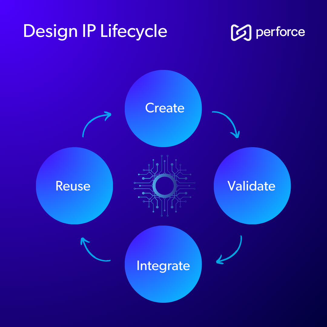
With growing SoC complexity, increased market demand, and the rapid pace of innovation, carefully managing both in-house and third-party IPs across the IP lifecycle is critical for staying competitive. Adopting an IP-centric approach to SoC development can reduce time-to-market and increase chip reliability by streamlining the design process and enabling effective reuse of previously validated designs.
In this guide, we explore what IP design entails, its importance, and how to effectively implement IP-centric strategies that accelerate and improve your semiconductor development. For a more personalized experience, talk to one of our IPLM experts about your workflow challenges and goals.
Back to topWhat Is Design IP?
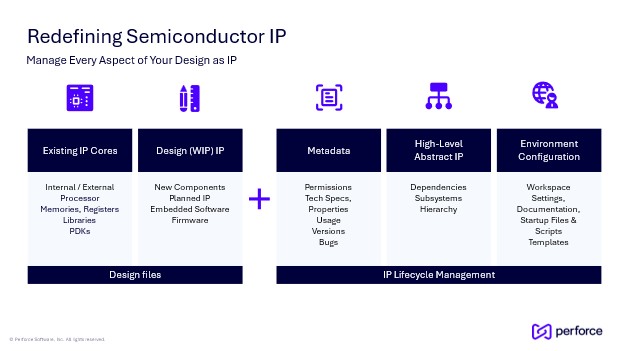
Design IP refers to the intellectual property components used in chip or system on chip (SoC) design. These could include hardware designs, firmware components, software libraries, and even CAD environments.
SoC design has changed dramatically in recent years. Previously, companies relied on custom, in-house designs with occasional third-party IP integration. Today, the majority of the SoC is platform-based or uses third-party IP. This approach allows companies to develop a family of products based off a single chip design with only small customizations to differentiate each product.
As a result, top semiconductor companies carefully manage, configure, and integrate their IPs so that they optimize operational efficiency, minimize design risk, and bring products to market faster.
Back to topExplore IP-Centric Design
Our technical white paper — The Transformation Model for IP-Centric Design — details how to use Perforce IPLM to manage design IPs and cut out the inefficiencies that slow development.
Why IP-Based SoC Design is Key
Design IP is crucial for quick product development when navigating complex ecosystems and managing risks to your SoC architecture.
That’s why it’s important to take an end-to-end view of your IPs in a transparent, traceable manner, using an IP lifecycle management application like Perforce IPLM (formerly Helix IPLM).
5 Key Challenges to Address with IP Management
- Version Sprawl: IP versions can quickly proliferate across design teams, increasing the risk for inconsistency and errors.
- Lack of Traceability: It becomes difficult to determine who used what IP, where, and when.
- IP Vendor Dependencies: External IP introduces licensing constraints, update delays, and quality concerns.
- Compliance and Audit Risks: Without clear traceability and documentation, meeting ISO 26262, ISO 9001, or internal audit requirements becomes costly.
- Fragmented Toolchains: IP is often handled outside the scope of traditional PLM or ALM systems, creating silos.
Related blog: Integrating PLM with IPLM to Optimize IP Semiconductor Lifecycle Management
Back to topHow to Transition to IP-Centric Semiconductor Design: 3 Steps
As the semiconductor design process evolves, here are steps to put IP first and keep your teams on the same page:
1. Clearly Define and Classify IP
Create a complete IP inventory by cataloging and categorizing all existing IP. Use a dedicated platform like Perforce IPLM to manage project IPs efficiently and thoroughly.
- Include functional blocks built in-house or purchased from third party vendors.
- Catalog less traditional IP design blocks and metadata, such as scripts, CAD files, or design templates.
- Manage all metadata (version history, dependencies, etc.) associated with each IP.
- Establish naming conventions, tagging rules, and quality gates.
- Create workflows for review, approval, and retirement of IP blocks.
- Limit access to IP by team, role, or geography based on licensing and security requirements.
- Ensure third-party IP is only used in approved locations.
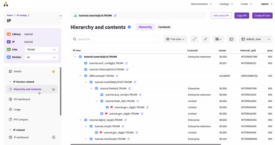
2. Build Hierarchical Dependencies
Once you’ve defined your IPs, you’ll need to build hierarchical dependencies. By mapping these hierarchies and implementing automated, hierarchical release mechanisms through a system like Perforce IPLM, IP teams will be better equipped to manage complex workflows and preempt design challenges.
- Map top-level system IP to subsystem components.
- Document IP dependencies across hardware, software, and firmware.
- Structure systems with reusable, modular parts to streamline integration.
- Prioritize critical dependencies to avoid cascading delays.
- Automate the IP release process, based on design dependencies, to ensure that IP blocks are released in the correct order, for quality-driven release flows.
- Visualize the hierarchy with flowcharts, Gantt charts, or dependency graphs to map out the relationships.
- Monitor and adjust as the system evolves and dependencies change.
3. Unify Data Management
To avoid inefficient and inconsistent data siloes, you’ll want to integrate and unify your IP design with a robust, scalable data management system.
Given the diverse needs of your design and development teams as well as the needs of your project, your organization may have multiple data management systems in play. Design teams may need to collaborate with embedded software developers who use Git, but it may be difficult to scale Git beyond source code.
Perforce P4, however, easily scales to meet the needs of complex SoC development. Plus, P4 offers a path to unify data management and bring Git projects into your pipeline via P4 Git Connector. Both P4 and P4 Git Connector fully integrate with Perforce IPLM.
This delivers a unified, single source of truth that allows you to:
- Manage the complex file relationships found in semiconductor designs.
- Handle large binary files and the millions of other files common in EDA tools.
- Automatically track changes, usage, and dependencies across all projects.
- Provide trace links from IP blocks to test results, documentation, and product releases.
- Identify frequently reused or underutilized IP.
- Use dashboards and analytics to highlight reuse opportunities and reduce redundant development.
Together, these tools provide a powerful solution to integrate and unify your IP-centric design with your data management system. To get the most out of your workflow, ensure all teams are properly trained in the best practices and that engineering, legal, and business teams are aligned on compliance and reuse goals.
Additional Resource: 5 Essential IP Governance Processes to Ensure Semiconductor Quality
Back to top6 Trends in IP-Centric Design: Futureproof Your Semiconductor Design Flow
As you move to an IP-centric design model, stay ahead of industry changes by embracing new technologies and methodologies. Here are some key trends to be aware of:
1. GenAI for Semiconductor Design
AI is poised to change semiconductor design but significant barriers stand in the way of full implementation. Without proper governance around IP origin and security, you risk costly errors or compliance failures. A bespoke platform like Perforce ALM provides a secure foundation to incorporate AI into your semiconductor design flow.
2. Open-Source and Vendor IP Collaboration
Open-source IP allows companies to collaborate and build on shared resources while reducing costs and fostering innovation. Collaborative third-party IP platforms offer controlled environments where vendors and licensees can exchange IP securely—with version tracking, licensing metadata, and digital fingerprints.
3. Advanced Security Measures for IP
As IP theft and cyberattacks become more common, companies must invest in IP security solutions, such as encryption, digital watermarking, and tamper-evident logging to protect their intellectual property.
4. IP Geofencing & Export Control
Enhanced governance features like region-based access restrictions, audit logs, and licensing controls ensure IP compliance with international regulations, especially critical in defense and automotive sectors.
5. Edge-Aware and Cloud-Based IP Management
Hybrid workflows have led to the proliferation of edge computing and cloud-based IP management tools. Cloud-based IPLM enables distributed teams to access IP assets in real time, while maintaining consistency and security across environments.
6. Sustainability in Semiconductor Design
Companies committed to environmental, social, and governance (ESG) goals use sustainable design practices such as reusing validated IP blocks. This reduces the need for rework and redundant tapeouts and saves time, energy, and resources. Modern IPLM platforms also support sustainability reporting by tracking reuse metrics and resource optimization.
Back to topAdopt IP-Centric Semiconductor Design with Perforce IPLM
Siloed design information, lack of traceability, and manual release flows lead to errors and extended timelines. Avoid these pitfalls with the tool designed specifically to manage IP across the design lifecycle: Perforce IPLM.
The Benefits of Using Perforce IPLM for IP Design in SoC
Perforce IPLM offers comprehensive traceability, IP release automation, a robust IP catalog, support for analog and digital IP, parent-child aware defect tracking, a hierarchical bill of materials, and configurable dashboards. Additionally, it delivers numerous benefits to large teams managing complex semiconductor design projects:
Benefit | Description |
Time-to-market | Pre-validated, reusable IPs mean faster design and integration cycles. |
Quality & reliability | Reduce the risk of bugs for more predictable verification and validation. |
Traceability | All IPs and metadata are tracked from block level to hierarchical BoMs. |
Innovation | A centralized IP repository means less time searching for IP and more time innovating. |
Efficiency | Faster workspace creation time gives designers instant access to the files and data they need. |
Collaboration | Teams across sites gain shared, secure IP access and real-time updates. |
Cost | Cut development costs and licensing overhead for third party IP. |
Compliance | A traceable IP ecosystem satisfies regulatory requirements with minimal effort. |
Scalability | Modular IP libraries scale with your projects and team size. |
Security | Role-based and geo-based access plus granular permissions protect your IP. |
Visibility | Configurable dashboards for more informed design decisions. |
Complete lifecycle management for your IP from ideation to delivery. | |
Change management | Complete records when IP blocks are modified, reused, or deprecated. |
“Having the capability to rapidly verify and integrate IP in current and future designs helps us differentiate and beat competitors to market.” - Top Semiconductor Firm
Take the next step and talk to a Perforce IP expert today. We’ll discuss your use case and how Perforce IPLM fits into your development process. If you’d like to learn more about following an IP-centric approach to SoC design, watch our webinar: 5 Steps to Achieve IP-Centric Design.
Related Reading on IP Design
Explore additional semiconductor topics: