Blog
April 29, 2026
What Is IP Core? Types, Lifecycle, and Reuse Strategies for Semiconductor

Embedded Systems & Chip Design
In modern chip development, an IP Core (semiconductor intellectual property core) is a reusable design element that reduces rework and speeds time to market. IP cores are often used for common functions like interfaces, controllers, and processors.
In this guide we’ll distinguish between soft, firm, and hard IP Core and highlight their benefits and shortcomings. We’ll also look at how to instill trust, improve quality, and keep projects on schedule through proper IP management. Additionally, we’ll explore the value of a dedicated IP lifecycle management tool like Perforce IPLM to govern IP safely, securely, and efficiently.
Back to topWhat Is an IP Core?
An intellectual property core, or IP core, is a block of logic or data that is used in the creation of a semiconductor chip. It typically belongs to a particular person or company but can be licensed for use by others.
IP cores range from simple components like an adder or a memory block to complex systems, such as a full processor (e.g., an ARM or RISC-V core) or a communication interface (e.g., PCIe or Fibre Channel). They can be developed in-house during the design process or purchased from third-party vendors. Today, over 100 companies develop and sell IP cores across analog, digital, and RF domains.
IP cores are commonly used in the creation of:
- Field Programmable Gate Arrays (FPGAs)
- Application-Specific Integrated Circuits (ASICs)
- System-on-Chip (SoC) designs
- Any other digital, analog, or mixed signal integrated circuit
What are the 3 Types of IP Cores?
IP cores are categorized as either soft, firm, or hard. The type of IP core you use influences everything from performance and flexibility to portability and development timelines. Here is how each type of IP core is defined along with its benefits and best use cases:
1) Soft IP Cores
Soft IP cores are typically delivered as synthesizable HDL/RTL (e.g., Verilog/ VHDL/ SystemVerilog) and implemented in the programmable logic or standard-cell flow.
Characteristics & Benefits:
- Highest flexibility: Easily modify and adapt code to specific needs
- Portable: Map to multiple technologies
- Customizable: Adjust during physical design
Trade-Offs:
- Performance is less predictable
- Results depend on synthesis, placement, and routing
- Most vendors do not offer support or warranty for modified designs
Use Cases:
- Designs that require portability across FPGA families, SoCs, or ASIC processes
- Projects where teams expect to customize or parameterize functionality
- Early‑stage designs where architectural flexibility is more important than final performance optimization
Examples:
- A soft processor core (such as a configurable RISC‑V CPU delivered as RTL) integrated into an FPGA design
- A custom DMA engine or protocol controller provided as HDL and tuned for different system requirements
2) Firm IP Cores
A firm IP core is usually delivered as a gate‑level netlist. It represents logic that has already been synthesized and optimized but lacks a fixed physical layout.
Characteristics & Benefits:
- More optimized and secure: Outperforms soft IP cores with better predictability and power
- Balanced: Provides a middle ground between reuse and IP protection
- Availability: Often provided by major FPGA vendors like AMD or Intel
Trade-Offs:
- Less flexible than soft IP cores
- More difficult to customize but easier to integrate than fully hardened IP
- Analysis and debugging can be more difficult without full source visibility
Use Cases:
- When you want more predictability/optimization than raw RTL provides but still need integration into your flow
- When IP vendors need stronger protection than editable HDL provides, while still delivering a reusable logic block
Examples:
- A memory interface controller delivered as a gate‑level netlist, optimized for timing but still integrated into a larger SoC flow
- A firm DSP block where the vendor wants to ensure consistent behavior while allowing limited integration flexibility
3) Hard IP Cores
Hard IP cores have both the logic implementation and physical layout fixed for a specific process technology or FPGA family. They are pre-mapped, pre-tested, and ready to drop into a design.
Characteristics & Benefits:
- Reliability: Provides the highest and most predictable performance
- Versatile: Fully supported by most foundries and silicon nodes
- Efficiency: Easy to integrate as pre-verified blocks
Trade-Offs:
- Designers cannot significantly alter the function after fabrication
- Analog hard IP cores (e.g., DAC, ADC, SerDes, PLLs) are provided in transistor-layout format. Digital hard IP cores are provided in layout format.
- Architecture around Hard IP must be determined early in the design
Use Cases:
- When you need maximum performance, power, and area (PPA) and can accept limited portability across families/nodes
- Common for specialized analog/mixed-signal and high-speed blocks where predictability is critical
Examples:
- High-speed transceivers
- Dedicated memory controllers
- RM cores in AMD's Zynq and Versal FPGA families
Back to top
Soft, Firm, and Hard IP Core Comparison Chart
| Aspect | Soft IP Core | Firm IP Core | Hard IP Core |
| Definition | Synthesizable HDL (Verilog/ VHDL) easily implemented for different technologies | Netlist or constrained RTL with mostly fixed logic | Fixed physical macro/layout for a specific process or device |
| Benefits |
|
|
|
| Shortcomings |
|
|
|
| Use Cases |
|
|
|
| Examples |
|
|
|
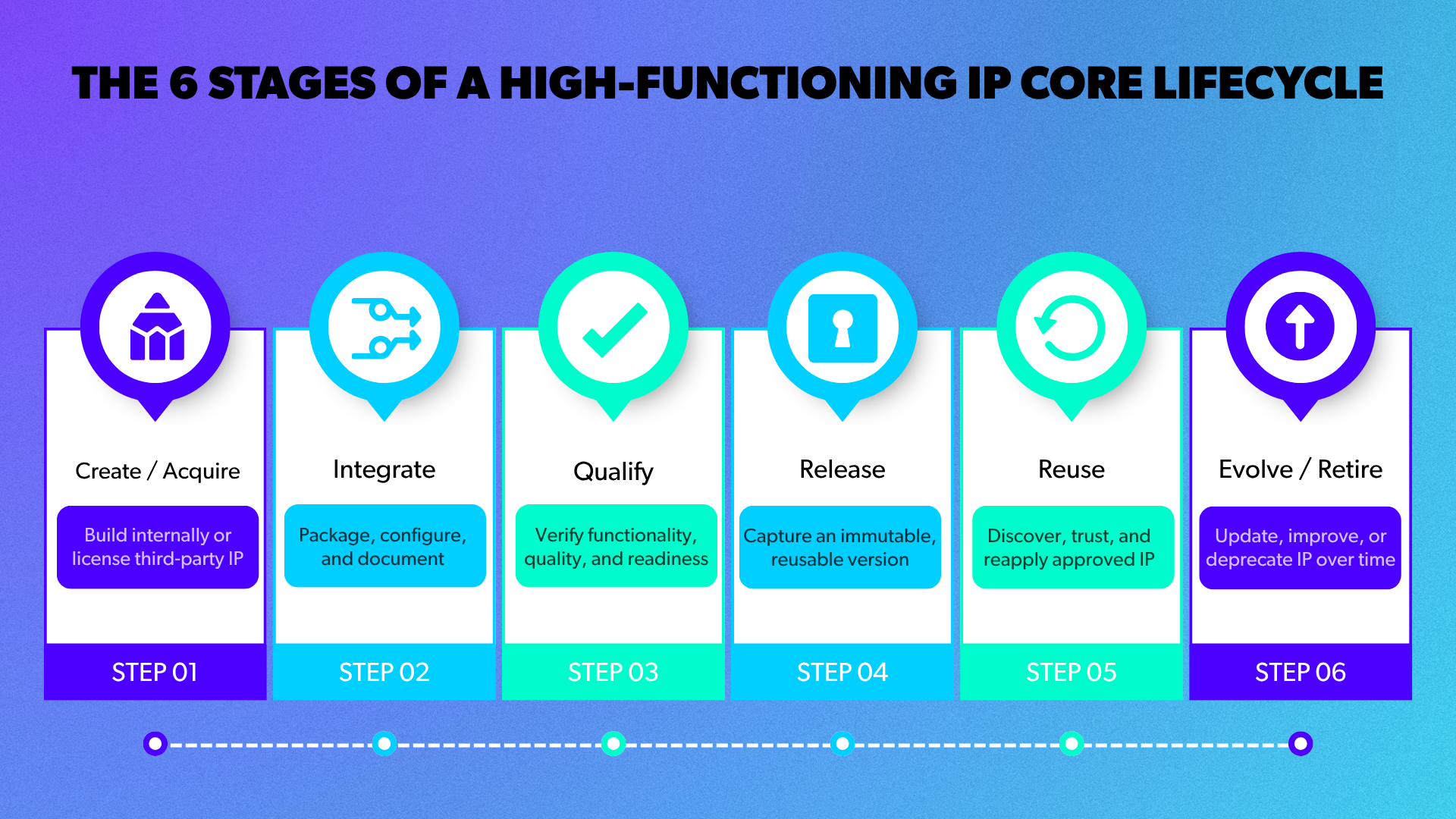
6 Steps of IP Core Development
Creating safe, functional, reusable IP blocks requires a clearly defined lifecycle from design to retirement.
1) Create or Acquire
The development process begins by creating the IP core from scratch or acquiring it from a third-party vendor. This step involves careful evaluation to ensure the IP meets required specifications and standards (owner/vendor, intended use, constraints).
2) Integrate
Once obtained, integrate the IP core into the overall chip design. Ensure compatibility with other components and address potential integration challenges by packaging the IP with interface expectations, clock/reset requirements, constraints, test collateral, and integration notes.
3) Qualify
The next step is rigorous testing and verification to qualify the IP core for use. This includes functional, performance, and compliance testing to ensure the IP is reliable and meets design criteria such as verification status, known issues, supported targets/nodes, and the conditions under which results are valid.
4) Release (the turning point)
This is where high-performing organizations separate work-in-progress from reusable assets. A good release is versioned, immutable, and reproducible so that teams can rebuild the exact design state later. At this stage, proper documentation and support materials are provided to facilitate implementation.
5) Reuse
To maximize efficiency, the IP core is designed with reusability in mind. However, reuse is only fast when discovery is easy. Engineers must be able to quickly find “the right IP” and understand its dependencies, quality, and usage history.
6) Evolve or Retire
Over time, IP cores may need updates to meet new requirements or evolving standards. These changes should occur under controlled workflows with strict change management and controlled access to protect sensitive IP and mitigate misuse. Outdated IP cores might be retired if they no longer provide value or meet modern design needs.
💡Additional Resource: For more on IP quality assurance through a governance lens, see: 5 Essential IP Governance Processes to Ensure Semiconductor Quality.
Back to top5 Benefits of Reusing IP Cores
Reusing IP cores, either internally developed or sourced from third parties, delivers measurable benefits across the design cycle:
- Faster time to market: Pre-verified blocks eliminate redundant design work.
- Lower development costs: Teams spend fewer engineering hours rebuilding existing functionality.
- Reduced technical risk: Proven IP cores have already been tested and validated.
- Improved quality: Well-maintained IP cores carry a track record of reliability.
- Greater design focus: Engineers can concentrate on the unique, differentiating aspects of their products.
For semiconductor organizations, the shift from a project-centric approach to an IP-centric approach is a strategic move that compounds these benefits over time.
Back to topThe Hidden Cost of Poor IP Core Governance
The impact of unmanaged IP cores is often hidden because problems appear incrementally across projects and teams. In practice, organizations commonly experience:
- Repeated re- verification cycles due to unclear usage conditions
- Schedule slips caused by late discovery of incompatible IP versions
- Redundant development when teams unknowingly rebuild existing IP
- Increased ECO churn triggered by unexpected IP behavior
- Higher tape out risk due to uncertain provenance or qualification gaps
Over time, these issues compound—slowing innovation and increasing risk across product families. High performing organizations address this by managing IP as a governed asset, not a project artifact.
Back to top3 Challenges When Managing Semiconductor IP Core as an Asset
IP management is a difficult, complex process with three core challenges: visibility, accessibility, and context.
1. Limited Visibility
Once an IP core is created and used in a design, it often ends up archived on a server with limited documentation. Without a centralized system, finding and reusing an existing IP core is nearly impossible. Teams either duplicate work unnecessarily or spend hours researching IPs they can't fully evaluate.
2. Poor Accessibility
Even when an IP core can be found, accessing it correctly often depends on institutional knowledge. You must clearly know which colleague worked on it, what version was used, and whether it's still fit for its intended purpose. That kind of knowledge rarely scales effectively and results in further bottlenecks.
3. Complex Context
Understanding an IP core means understanding the full context of the IP: Which projects has it been used in? How has it evolved? Are there outstanding bugs that impact it? As organizations move from a project-centric to an IP-centric design approach, building that full contextual picture becomes critical.
Back to topHow to Manage IP Cores successfully
A dedicated IP management platform like Perforce IPLM directly addresses these visibility, accessibility, and context challenges. It provides a scalable IP lifecycle management platform that tracks IP cores and their associated metadata across projects with end-to-end traceability.
The result: Perforce IPLM streamlines IP reuse so that design teams spend less time searching for or duplicating IP cores and more time moving the project forward.
Back to topWhat If Everything Could Be Managed Like IP?
Defining IP to just the cores in your chip design limits their reuse. With Perforce IPLM, anything can be managed as an IP, including:
- Engineering environments and configurations
- Work-in-progress (WIP) IP
- PDKs and libraries
- Usage tracking
- Extensions
- Release management artifacts
- Integrations
- IP generators
- And more
You can also apply labels to indicate IP cores from specific vendors, flag exact compliance standards, set granular permissions, and include notifications when an IP changes. Organize your IP into hierarchies or workspaces and release immutable IP Versions (IPVs) for repeat use.
Back to topIP Core and Metadata
Without metadata for every IP, teams can’t confidently answer basic questions around their origin and integrity. With IPLM, you can maintain up-to-date metadata in the following categories:
| Category | Meta Description |
| Ownership & Provenance | Where it came from – internal owner/ third-party vendor |
| Delivery & Constraints | Soft/firm/hard, target devices/nodes, key constraints |
| Interfaces & Integration | Expected buses/ports, clock/reset assumptions, integration notes |
| Verification & Quality | Status, test collateral, known issues/errata |
| Dependencies & Composition | What child IPs it includes and what it requires |
| Usage & Impact | Which projects used it and what changed across versions |
| Security & Access | Who can view, integrate, or modify it (and who should be notified when it changes) |
A Centralized Bill of Materials for Semiconductor IP
A central semiconductor IP management platform that operates independently of your data management tool is key to creating a Bill of Materials (BOM). It provides a complete record of how IPs are used across your organization and supports both IP discovery and systematic reuse across software, hardware, and firmware.
Perforce IPLM includes Component and IP Bill of Materials (CIPB) capabilities that work alongside your ERM and manufacturing-focused PLM tool to:
- Provide high-level data on IP that matches your design specifications
- Support hierarchical planning across both third-party and internal IP
- Deliver a unified, consolidated BoM to manufacturing
- Give teams a holistic view of software, firmware, and hardware IP
Together, these capabilities help design organizations maintain consistency across the entire semiconductor IP design process, from initial planning through final tape-out.
Back to topImprove Semiconductor IP Management
IP lifecycle management is a force multiplier. When IP is managed centrally and consistently, organizations unlock benefits that extend beyond reuse alone:
- Teams onboard faster
- Integration issues surface earlier
- Institutional knowledge is preserved across generations of products
Over time, this allows each new program to begin with a stronger, more trusted IP foundation. It compounds efficiency and reduces risk release after release.
Discover why 9 of the 10 top semiconductor companies trust Perforce IPLM for efficient, traceable, and secure workflows.
Connect with one of our experts for a personalized demo that illustrates how Perforce IPLM can manage your IP cores for greater efficiency and reliability.