Blog
December 4, 2025
Integrating Electronic Design Automation (EDA) Tools with IP Lifecycle Management

Embedded Systems & Chip Design
The right electronic design automation (EDA) software can help semiconductor design teams meet tight time-to-market deadlines, lower costs, and avoid the immense cost of errors. Using EDA tools, you can:
- Streamline and automate chip design.
- Simulate how circuits will perform.
- Test and verify design elements.
A recent Business Wire report anticipates that as the semiconductor industry grows more competitive and new chip technology emerges, the market for EDA tools will skyrocket to $22 billion in 2030.
In this guide, we’ll define what electronic design automation software does, outline the EDA workflow, and discuss how it solves common industry pain points. Additionally, we’ll look at how IP and data management solutions like Perforce IPLM and Perforce P4 support popular EDA tools to streamline, scale, and secure semiconductor design workflows.
Ready to see how Perforce IPLM and P4 can enhance your electronic design automation processes?
Back to top
What Is Electronic Design Automation?
Electronic design automation brings together software, hardware, and services to plan, design, and verify semiconductor designs. EDA tools ensure chip designs meet all requirements before fabrication.
Modern semiconductor design—particularly complex system-on-chip and chiplet-based design approaches—would be impossible without a high level of electronic design automation. EDA tools power chip design for an increasingly wide array of industries, from automotive and consumer electronics to aerospace technology and telecommunications.
Back to topThe Role of EDA Tools for Semiconductor Design
Electronic design automation (EDA) tools are software solutions that enable engineers to design, simulate, and verify complex circuits with precision and efficiency. They allow teams to predict semiconductor behavior, assemble circuit elements, and anticipate chip performance.
Companies like Synopsys, Cadence, and Siemens have been at the forefront of the electronic design automation marketplace and its continued innovation since the 1960s. While the EDA workflow has grown exponentially in complexity and tooling since then, the core functions of EDA tools can be simplified into three key phases:
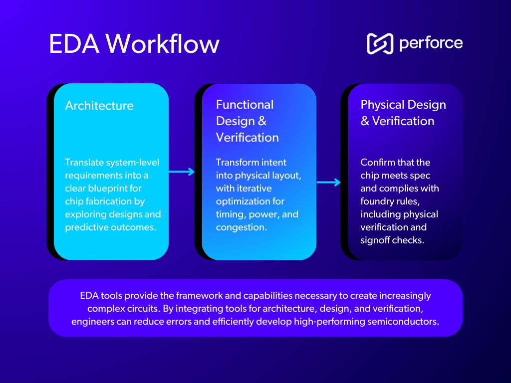
The EDA Workflow: Three Stages of Semiconductor Development
EDA workflows are best understood in three core stages:
- Architecture
- Functional design & verification
- Physical design & verification
Each stage is critical to achieving high performance, reliability, and manufacturability. Below are detailed insights into each phase, the processes involved, and the tools that make success achievable.
1. Architecture
The architecture stage defines the scope of a semiconductor project. It involves translating system-level requirements and design intent into a clear blueprint for execution.
In this foundational phase, EDA tools play an increasingly vital role, moving beyond simple capture to enabling sophisticated analysis and optimization that directly impacts the project's success. These tools allow architects to explore a vast design space, validate architectural choices, and predict performance before committing to costly downstream implementation.
Processes Involved:
- Specification & Requirements Capture: Translate marketing, customer, and application needs into quantifiable design goals.
- System and Chip-Level Architecture Definition: Determine compute, memory, interface, and power architecture.
- High-Level Design Exploration: Evaluate tradeoffs using modeling languages (SystemC, TLM), architectural simulation, and early power/performance estimation.
Typical Tools:
- System Modeling: Simcenter System Architecture, MATLAB/Simulink, SystemC,
- Architectural Simulators: Synopsys Platform Architect, Cadence Stratus HLS
- Specification Tools: Requirements management platforms, IP cataloging solutions
2. Functional Design & Verification
Once the architecture is set, engineering teams implement the system’s functions at the Register-Transfer Level (RTL) and validate functional correctness through comprehensive verification strategies.
Design EDA tools take a proposed circuit function and assemble the elements needed to build it. These solutions provide both physical and logical direction. Design EDA tools help teams create the right geometric shapes and give insight into how to connect these integral components. Usually overseen by a designer, this process is also referred to as “place and route” or a custom layout. The goal is to ensure correctness before physical implementation.
Processes Involved:
- RTL Design & Coding: Transforming architecture concepts into VHDL, Verilog, or SystemVerilog code.
- Functional Verification: Deploying simulation, formal analysis, and coverage-driven validation.
- Testbench Development: Building modular, reusable test environments.
- Early Power, Performance, and Area (PPA) Analysis: Using early estimates to inform optimization before physical implementation.
Typical Tools:
- RTL Development: Synopsys Design Compiler, Cadence Genus, Siemens Questa
- Simulation: Synopsys VCS, Cadence Xcelium, Siemens ModelSim
- Formal Verification: Cadence JasperGold, Synopsys VC Formal
- Coverage & Debug: Verdi, SimVision
3. Physical Design & Verification
In the final stage, the functional RTL design is converted into a manufacturable layout. This process relies heavily on EDA tools to automate and optimize complex tasks. For example, Place and Route tools efficiently position gates and standard cells on the silicon die and establish the thousands or even millions of interconnections involved, all while meeting strict requirements for timing, area, and power.
Physical verification tools then ensure that the layout complies with foundry manufacturing rules and verify that it is both physically manufacturable and electrically accurate. Throughout this stage, teams focus on optimizing timing, area, and power while rigorously validating the design’s integrity against foundry specifications.
Processes Involved:
- Synthesis: Converting RTL to gate-level netlists.
- Place and Route: Physically arranging components and wiring connections on silicon.
- Static Timing Analysis (STA): Verifying timing constraints are met.
- Physical Verification: Running Design Rule Checks (DRC), Layout vs. Schematic (LVS), and Electrical Rule Checks (ERC).
- Signoff: Final compliance with foundry/industry manufacturing rules.
Typical Tools:
- Synthesis & P&R: Synopsys Fusion Compiler, Cadence Innovus, Siemens Aprisa
- Timing Analysis: Synopsys PrimeTime, Cadence Tempus
- Physical Verification: Siemens Calibre, Synopsys IC Validator, Cadence Pegasus
Power Analysis: ANSYS RedHawk, Synopsys PrimePower
Speed Up Time to Market with EDA Tools + IP-Centric Design
Pairing electronic design automation software with an IP-centric approach can empower your team to work more efficiently. Our Transformation Model for IP-Centric Design whitepaper details how placing IP at the center of your design process can help you get to market faster than the competition and reduce costly re-spins. Plus, it breaks down the five-step process organizations can follow to achieve this transformation.
Back to topHow Perforce Addresses the Challenges of Electronic Design Automation
While electronic design automation is indispensable for the semiconductor industry, these tools come with their own set of obstacles and risks:
Development Cycle Complexity
Large, dispersed teams, intricate chip systems, and complex IP versions and dependencies place increased demands on development teams and their leaders. The pressure to move products to market without costly re-spins and product delays means using the right tools and processes out of the gate.
Perforce Solution:
Perforce IPLM provides a centralized workspace that allows you to manage your IP with robust search and filtering capabilities across multiple users. It easily integrates with Jira to track issues and meet quality and maturity approvals, all within a single platform.
IP Security and Compliance Concerns
Distributed design teams, external IP vendors, and shifting export regulations mean securing design IP blocks is a top priority. However, without a strong investment in automation, centralization, and collaboration tools, engineers often struggle to implement consistent safeguards and best practices.
Perforce Solution:
Teams can proactively defend against IP leakage with granular permissions and geofencing capability within Perforce IPLM. Additionally, Perforce IPLM can help semiconductor organizations ensure that they meet fab security requirements by providing a single source of truth that teams can use to establish an immutable, hierarchical bill of materials.
📕Related Content: IP Geofencing With Perforce IPLM
Maintaining Traceability for IP Reuse
With an increasing focus on reusing IP blocks, engineers must maintain clear traceability between design components, their versions, and verification results. Poor management of IP provenance can lead to integration issues, rework, and compliance risks.
Perforce Solution:
An IP lifecycle management solution like Perforce IPLM records every change to your IP while integrating with your existing electronic design automation infrastructure. With traceability in mind, every aspect of the IP lifecycle is visible in Perforce IPLM in easy-to-understand, configurable dashboards. Designers can see the projects the IP has been used in, any outstanding bugs, derivative designs, regression status, and much more. Complete IP management makes it easy to confidently reuse IP without the risk of using unverified components.
📕Related Content: Why Is Traceability Important?
Lengthy Verification Cycles
Verification is one of the most time-consuming phases in the design process. Engineers often struggle with slow coverage closure, incomplete test scenarios, and debugging regressions, which can lead to delays and missed deadlines.
Perforce Solution:
The right collaboration tools, like Perforce P4 data management, keep teams aligned and moving forward for a more efficient design cycle.
Working at Scale
Electronic design automation tools generate millions of design files, some of them hundreds of gigabytes in size. This can overwhelm some data management tools, slowing collaboration.
Perforce Solution:
To meet this challenge, teams need a data management tool with unlimited scalability, like Perforce P4. Perforce P4 integrates seamlessly with Perforce IPLM and is used by leading semiconductor companies like Samsung, NVIDIA, and Texas Instruments.
Back to top5 Future Trends: EDA Challenges and Solutions
Electronic design automation tools and processes have been a part of the semiconductor industry for more than 60 years. Geopolitical events, the rise of new technology, and consumer demand have long driven their development. Below are five key EDA trends designers currently face along with tips for getting ahead of them.
1. AI-Native EDA
Embedded AI and ML EDA tools will be increasingly used to automate verification, predict design outcomes, accelerate design cycles, and improve error detection.
Challenge: The increased file loads associated with automation along with security and provenance issues will make IP lifecycle management crucial in the age of AI.
How to Stay Ahead:
- Invest in team training on AI-enabled tools and ensure secure, governed access to high-quality data for effective model training.
- Establish governance frameworks for AI adoption to maintain transparency and trust.
- Pilot AI features in synthesis, verification, or debug now, to learn where it accelerates vs. where it needs human oversight.
- Treat AI outputs as versioned artifacts — store prompts, generated RTL, and test vectors in version control so results are reproducible.
📕Related Webinar: Building Trust in Gen AI for Semiconductor Design
2. Integration with Cloud-Based Tools
Migrating to cloud platforms improves scalability, reduces costs, and streamlines global collaboration on large chip projects. One EDA executive said almost all of his organization’s customers use cloud tools within their design process.
Challenge: While EDA tools work with cloud-based infrastructures, they may perform less efficiently. Organizations will need to prioritize their EDA tools’ performance in the cloud as the shift to cloud-based data management continues.
How to Stay Ahead:
- Define clear data movement policies. Only replicate necessary files and use caching/edge servers to minimize egress costs.
- Test workloads in cloud-native EDA flows (especially verification) so your team has experience scaling when project deadlines spike.
- Invest in version control that keeps designers and cross-functional teams in sync.
3. Advanced 3D IC and Chiplet Packaging
As Moore's Law slows, industries will shift towards 3D ICs, chiplet-based design, and advanced packaging technologies to meet performance and power requirements. This trend demands new EDA tools that address 3D design across multiple dies and maintains power integrity in stacked designs.
Challenge: With the rise in chiplets and 3D ICs, engineers must optimize logic, packaging, heat, and connections together. Testing must ensure components communicate correctly and that the packaging doesn’t cause problems.
How to Stay Ahead:
- Build expertise in chiplet and 3D IC design and adopt EDA solutions that support multi-die integration, packaging-aware workflows, and advanced simulation capabilities.
- Establish IP lineage tracking so every element of the design is hierarchically versioned and traceable.
- Create multi-domain collaboration channels (logic, package, board) with a single data backbone.
- Train engineers in universal chiplet interconnect express (UCIe) standards and 3D packaging tools early to shorten future adoption curves.
- Leverage reusable design IP to meet the demand for faster and more reliable complex system design.
4. Safety, Security, and Compliance by Construction
Safety, security, and compliance have always been paramount in semiconductor design. As more tools and technologies are introduced, measures must be taken to ensure design integrity and meet global compliance standards.
Challenge: Automotive (ISO 26262), aerospace (DO-254), medical, and industrial markets demand requirements traceability, change control, and air-tight verification. Plus, security concerns like IP integrity and hardware supply chain risks are rising.
How to Stay Ahead:
- Treat every artifact—requirements, test vectors, proofs, tool versions, constraints—as first-class, versioned metadata.
- Automate compliance with traceability reports that connect requirements → tests → results.
- Adopt secure access controls and signed IP policies to strengthen your design chain.
5. Sustainability in Chip Design
Power isn’t just a battery-life metric; it’s tied to thermal envelopes, cooling cost, and ESG goals. EDA tools now often feature power and security analytics to meet designer needs and optimize energy efficiency across the design cycle.
Challenge: Growing pressure for lower power consumption and reduce environmental impact, particularly in the IoT, edge, and mobile segments.
How to Stay Ahead:
- Incorporate energy-efficient design metrics into your workflows.
- Evaluate the environmental impact of design decisions.
- Stay informed about emerging tools and methodologies for sustainable design.
- Standardize power-intent files across teams and track them in version control.
- Make early power estimation part of every project milestone, not just late-stage analysis.
- Build sustainability metrics (like energy per operation) into your design KPIs.
Enhance Your Electronic Design Automation Approach with Integrated IP and Data Management
Across all these trends, the common threads are IP quality and provenance, secure collaboration, and scalability — the areas where Perforce’s integrated IP and design data management solutions shine:
- Perforce IPLM supports and enhances electronic design automation. While EDA infrastructure addresses common prototyping and testing challenges, IP management provides a unified data model that serves as a foundation and single source of truth for electronic design automation.
- Perforce P4 easily handles the millions of files common in EDA tools, including large binary files, and manages the complex file relationships found in semiconductor designs. Plus, it controls access down to the file level for enterprise-class security.
Discover why 9 of the top 10 semiconductor companies, including NVIDIA, Samsung, Texas Instruments, and others, rely on Perforce to:
- Qualify IPs to ensure they have been fully vetted and verified.
- Ensure end-to-end traceability from requirements to release to ensure regulatory compliance and understand the cross-project impact of known issues.
- Enable secure collaboration through a single source of truth for all design data, while protecting valuable IP.
- Scale endlessly, with seamless, nearly instantaneous file access for engineers and designers.
EDA tools represent a significant investment in your semiconductor design process. Ensure that you maximize your ROI with a foundation of IP and data management that supports your workflow.
Connect with a Perforce expert today to schedule a personalized demo and learn how Perforce IPLM and P4 can enhance your electronic design automation processes.